


 Seonglae Cho
Switch - Logical device
Planar → FinFET → GAA
Transistors
Transistor Notion
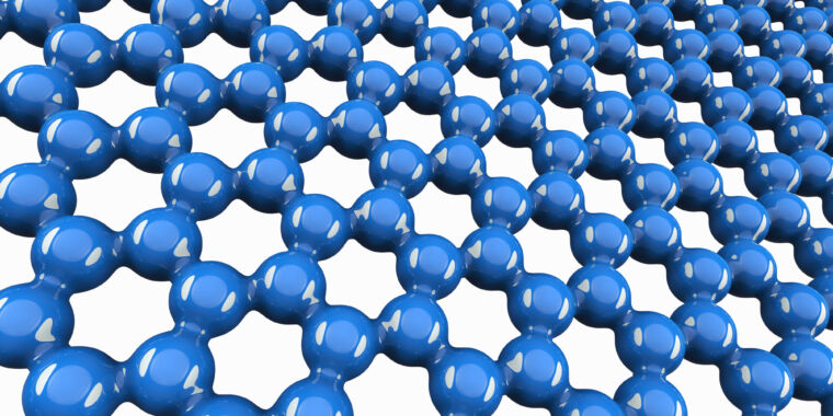
A transistor made using two atomically thin materials sets size record
The ever-shrinking features of transistors etched in silicon have always required pushing the cutting edge of manufacturing technology. The discovery of atomically thin materials like graphene and carbon nanotubes, however, raised the prospect of replacing our manufacturing needs with the natural properties of these materials.

https://arstechnica.com/science/2022/03/a-transistor-made-using-two-atomically-thin-materials-sets-size-record
몇 nm(나노미터)라는 건 어떤 부분을 말 하는 걸까?
오늘은 반도체 미세공정에서의 'nm'라는 게 실제로는 어떤 건지에 대한 내용을 전반적으로 다뤄봤는데요. 스탠다드 셀은 보통 Cell based design인 디지털회로설계에서 널리 쓰이고 있습니다. 그리고 후반부의 셀 사이즈 최적화는 DTCO에 대한 내용이고 Fin/Metal tr...

https://www.youtube.com/watch?v=ij6Rk8peX9Q

초 미세 반도체를 만드는 EUV의 원리를 쉽게 알려드립니다
차세대 반도체를 만드는데 꼭 필요한 EUV에 대해 간단히 설명했습니다.앞으로 얼마나 더 공정이 미세화 될지 저도 참 궁금합니다.CPU,GPU,메모리 등 미세 패터닝이 필요한곳에 EUV노광이 사용됩니다.#EUV#반도체#CPU00:00 Imtro00:32 배경설명02:36 EUV 만드...
https://www.youtube.com/watch?v=kmFfesriafM
